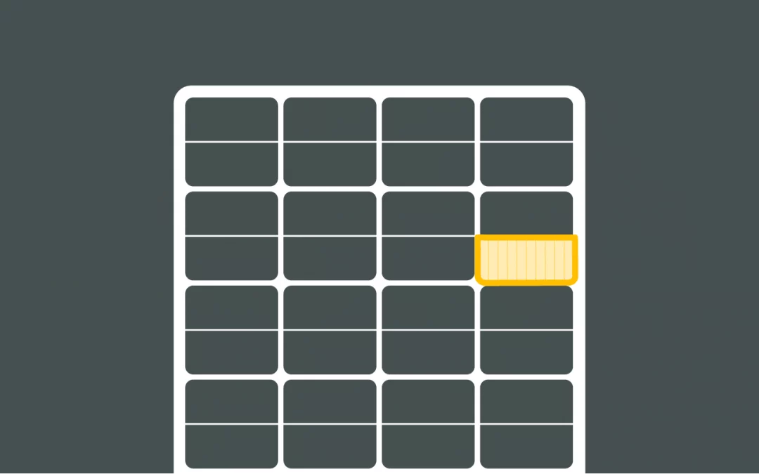
P-type and N-type technology differ
in the structure of the wafers
The underside of the wafer is positively charged and doped with boron, with one electron less than silicon.
On the other hand, the top side of the wafer is negatively charged.
The wafer is charged with Phosphorus doped and contains an electron
more than silicon.

The underside of the wafer is negatively charged and doped with phosphorus, with one electron more than silicon.
On the other hand, the top side of the wafer is positively charged.
The wafer is charged with doped with boron and contains one electron less than silicon.

The different structure of the wafers leads to a lower temperature coefficient in N-type cell technology and enables higher yields and significantly better long-term stability.
Solar Fabrik modules with N-Type technology
You can recognize which Solar Fabrik modules have N-type technology by the "N" at the end of the product name.


